"Step-by-step" example of an ExpressPCB project
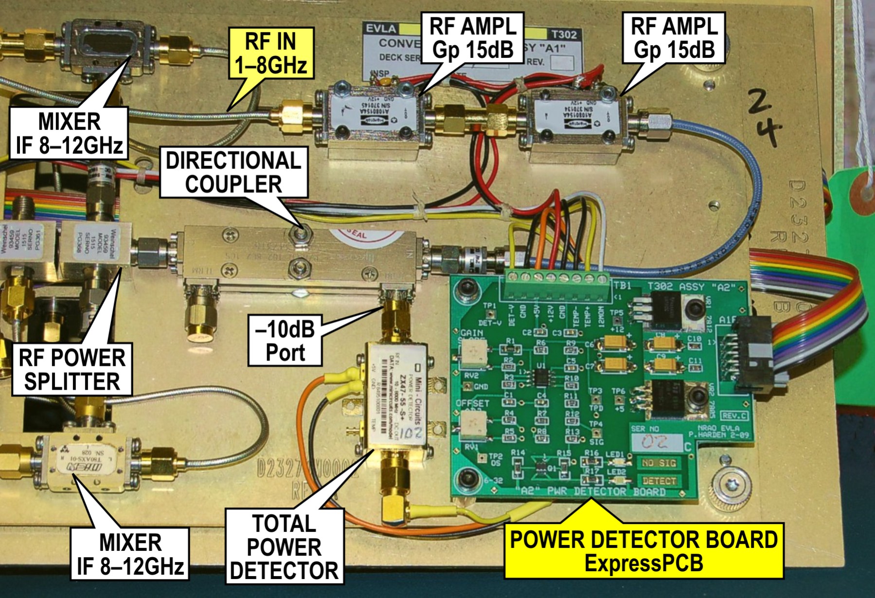
PROJECT: This was an ExpressPCB project I did at work. I was asked to add a total power detector (TPD) to our LSC band upconverter
modules (upconverts 1-4 and 4-8GHz to 8-12GHz IFs) used in the VLA antennas. The TPD (and directional coupler for sampling the power)
is placed after the RF amplifiers and before the mixers to measure input RF power and for diagnostics to ensure no previous stages
are in compression or the presence of RFI. The 1-8GHz power detector is a MiniCircuits component. A PCB was needed for the circuitry
to power the detector and scale the output to the 0-10v analog range used by our remote monitoring system. The boards were made by
ExpressPCB. The schematic, PCB layout and photos of the completed project are shown below as a "step-by'step" example of designing
a circuit, the PCB, getting the board made, and building it. This would be the same steps and procedures -- whether a job for work,
or a QRP project.
Click on all illustrations and photos to enlarge
Step 2 -- Draw the schematic diagram
(using ExpressSCH Schematic)
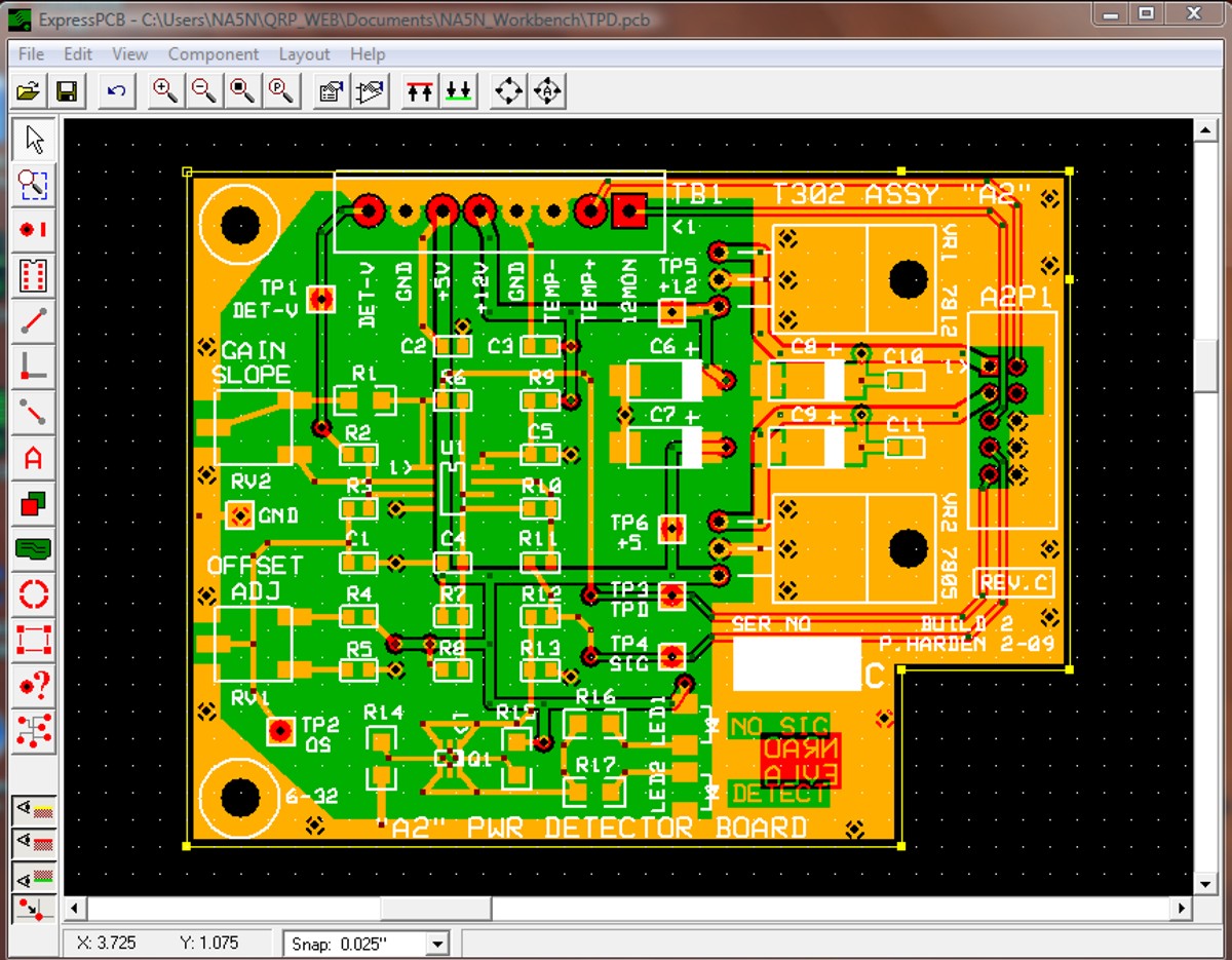
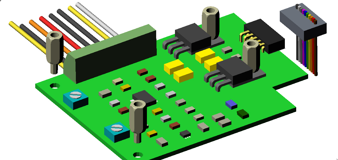
Step 3 -- Do the PCB layout
(using ExpressPCB layout)
Click here to load actual ExpressPCB schematic (NOTE: 11x17 size)
HINTS: Make sure all custom components you create have pin numbers. Run the "schematic check for net errors" under FILE for obvious
errors. As shown above, add explanatory notes, provided you don't use schematic components or wiring (use the line functions and text).
HINTS: Don't forget to link your PCB to the schematic under the FILE menu. You may have to create a custom footprint for any custom
schematic components you created; make sure you assign proper pin numbers per schematic component.
Step 4 -- Order the boards online
Step 1 -- Overall concept
If you've never made a PCB before, my first suggestion is to sit down and think it through carefully before you start drawing the
schematic and laying out the board.
1. Are you constrained to a certain board size? Do you need mounting holes?
2. What connectors,
interconnects, controls & indicators do you need?
3. Where should they be placed to properly integrate into your project?
4. Do
any of your components need heat sinking or separation from other parts?
Sometime it is advisable to sketch out your project,
visualize what it will look like, and make sure all dimensions (don't forget about height) are a proper fit. Simple mistakes,
like not allowing enough clearance for a part, wrong pin spacing used for a connector, or mounting holes in the wrong place can be
costly.
For this project . . . a 2-sided PCB was used as no RF is on the board for impedance concerns warranting a 4-layer board.
Most components are surface mount using 0805 resistors and capacitors. Most traces are .015 or .020" width.
For this project, the size of the board was fairly critical to fit within an existing piece of electronics. A scaled conceptual drawing
was used to "fine tune" the dimensions and determine critical parts placement before the board layout was begun.
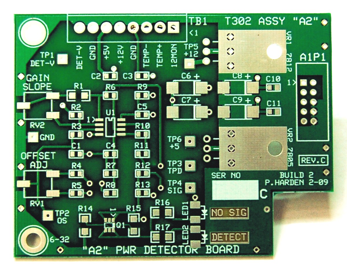
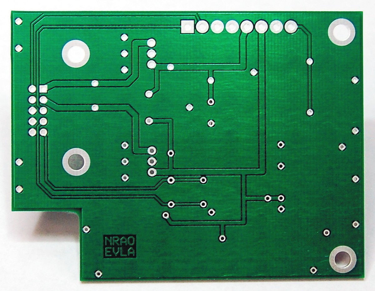
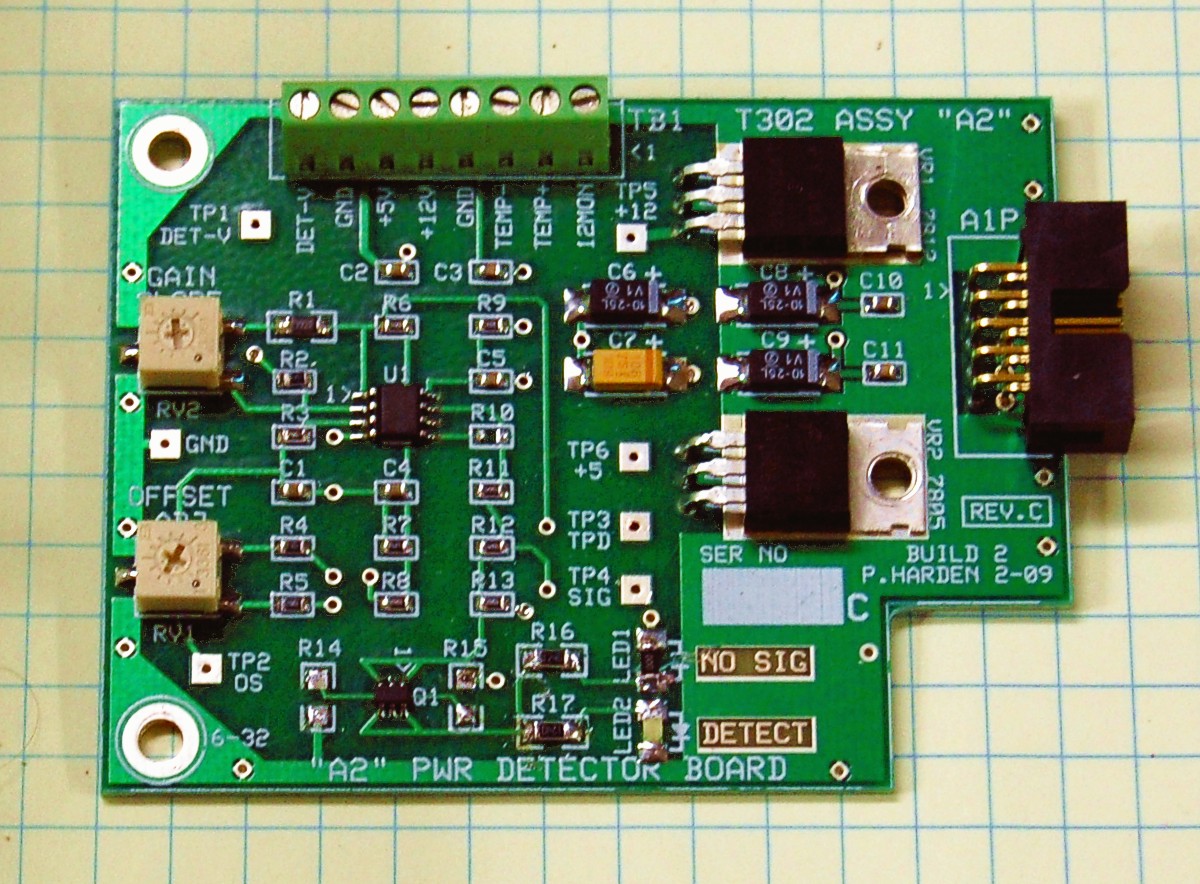
Step 5 -- Inspect board upon receipt
Check for any obvious errors; use ohm meter to verify open circuit between ground and your power runs; use magnifying glass to inspect for clean traces, no touching traces, etc. Inspect both TOP and BOTTOM sides.
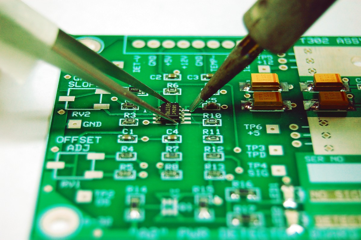
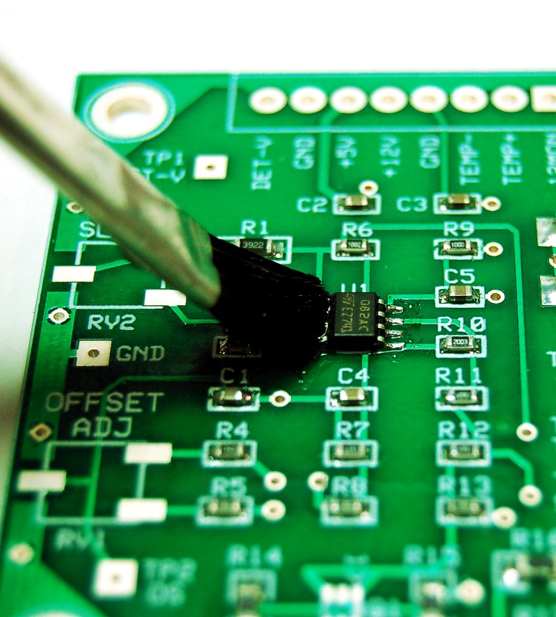
Step 6 -- Plug-in soldering iron; build board
Mount components and solder in place using standard building practices that have made QRPers famous. Clean solder with alcohol and a hobby brush to remove excess flux.
Step 7 -- Inspect completed board
Check that all components are installed. With magnifier, check soldering for splashes, bridges between pins or traces, or for too little or excessive solder on pads. Clean board with alcohol and a hobby brush to remove excess flux.
Step 8 -- Install finished board into project
Install the board, wire, apply power and smoke test (sorry, no smoke to photograph with this project!). The finished TPD and board is shown below installed in an operational module.
There are two total power detectors and PCBs in each LSC upconverter module (one for each polarization); there are 28 VLA antennas, a module for each antenna plus four spares for 32 total modules for 64 of these PCBs needed. Seventy of these boards were built for the project and to have a few spares. I built about 20 of them; technician Eric Chavez built the other 50.